Contents Catalog
- 1 Features of our GJL40B Crystal growth furnace
- 2 Applicable crystal of our GJL40B Crystal growth furnace
- 3 The role of the crystal growth furnace in the process of crystal formation
- 4 Related Equipment the crystal growth furnace
- 5 What are the methods for growing silicon carbide crystals?
- 6 Learn more and contact us
The crystal growth furnace GJL40B is mainly used for the crystal growth of semiconductor materials. By precisely controlling conditions such as temperature, atmosphere and mechanical movement, it achieves the growth of high-quality single crystals. This equipment occupies a crucial position in the semiconductor industry and is one of the key devices used in preparing high-performance semiconductor devices. The structure design of the crystal growth furnace GJL40B is precise. It mainly consists of the furnace body, heating system, vacuum system, atmosphere control system, mechanical motion mechanism and control system, etc. All parts work in coordination to ensure the stability and controllability of the crystal growth process.

Features of our GJL40B Crystal growth furnace
- Furnace body: It is made of high-strength, highly corrosion-resistant materials, capable of withstanding long-term operation under high-temperature and vacuum environments.
- Heating system: It adopts advanced heating technology and materials to provide a stable and uniform heating environment, ensuring the temperature conditions required for crystal growth.
- Vacuum system: It has high-efficiency vacuum pumping and pressure-holding capabilities, providing the required vacuum environment for crystal growth.
- Atmosphere control system: It can precisely adjust the composition and pressure of the atmosphere in the furnace to meet the needs of different crystal growths.
Applicable crystal of our GJL40B Crystal growth furnace

SIC CRYSTAL

SAPPHIRE CRYSTAL
more crystal wafers please click:https://www.goodwafer.com/
Silicon carbide single crystals are used in power electronic devices, optoelectronic devices, high-frequency devices, aerospace and military fields, as well as in the manufacture of wear-resistant cutting tools and high-temperature resistant materials due to their excellent physical, electrical and chemical properties.
Sapphire single crystals are widely used in optoelectronics (e.g., LED substrates), electronics (e.g., semiconductor wafers), optics (e.g., windows and lenses), aerospace (e.g., infrared domes), and precision instruments due to their high hardness
The role of the crystal growth furnace in the process of crystal formation
In the silicon carbide crystal growth process, the crystal growth furnace (long crystal furnace) serves as the core equipment to provide and precisely control the high-temperature environment (typically 2000–2500°C), thermal field distribution, gas flow (e.g., argon atmosphere), and pressure conditions required for vapor-liquid-solid phase transition, ensuring the stable nucleation and uniform growth of high-quality silicon carbide single crystals while minimizing defect formation.
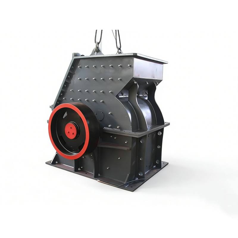
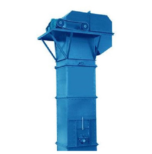
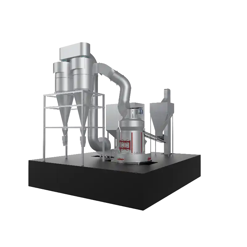
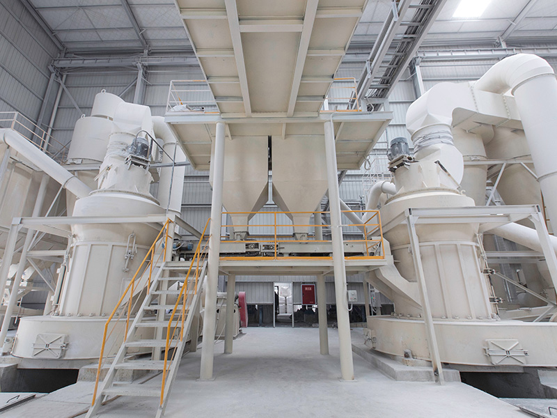
Related Equipment the crystal growth furnace


What are the methods for growing silicon carbide crystals?
Here are the main methods for silicon carbide (SiC) crystal growth and their advantages:
1. Physical Vapor Transport (PVT) Method
- Advantages:
- Widely used in industrial production for growing large-size SiC single-crystal substrates (up to 8 inches).
- Mature technology with stable performance, suitable for producing 4H-SiC and 6H-SiC substrates for power electronics and RF devices.
- Enables precise control of temperature, gas flow, and pressure to minimize defects like micropipes and dislocations.
2. Chemical Vapor Deposition (CVD) Method
- Advantages:
- Used for epitaxial layer growth on SiC substrates or heterosubstrates (e.g., Si, sapphire).
- Enables high-quality thin-film deposition with precise thickness and doping control, critical for fabricating semiconductor devices (e.g., MOSFETs, IGBTs).
- Compatible with both high-temperature CVD (HTCVD) for thick films and metal-organic CVD (MOCVD) for nanoscale heterostructures.
3. Liquid Phase Epitaxy (LPE) Method
- Advantages:
- Lower growth temperature (1600–1800°C) reduces thermal stress and defect formation.
- Faster growth rates compared to PVT, though solvent contamination risks require careful control.
- Suitable for laboratory-scale research on low-defect-density SiC (e.g., 4H-SiC) and specialized applications.
4. Vapor-Liquid-Solid (VLS) Method
- Advantages:
- Ideal for synthesizing one-dimensional SiC nanostructures (nanowires, nanorods) using metal catalysts (e.g., Au, Ag).
- Enables precise control over nanostructure morphology and orientation for nanodevices and composite materials.
5. Melt Growth Method
- Advantages:
- Directly melts SiC raw materials, potentially simplifying the growth process (though limited by SiC’s high decomposition temperature >2800°C).
- Remains a research focus for future large-scale, low-defect crystal growth.